

Nikon Launches DSP-110 Digital Lithography System with 1.5 µm Resolution
Semiconductor Back-End Process Lithography System that Achieves Approximately 40% Higher Throughput
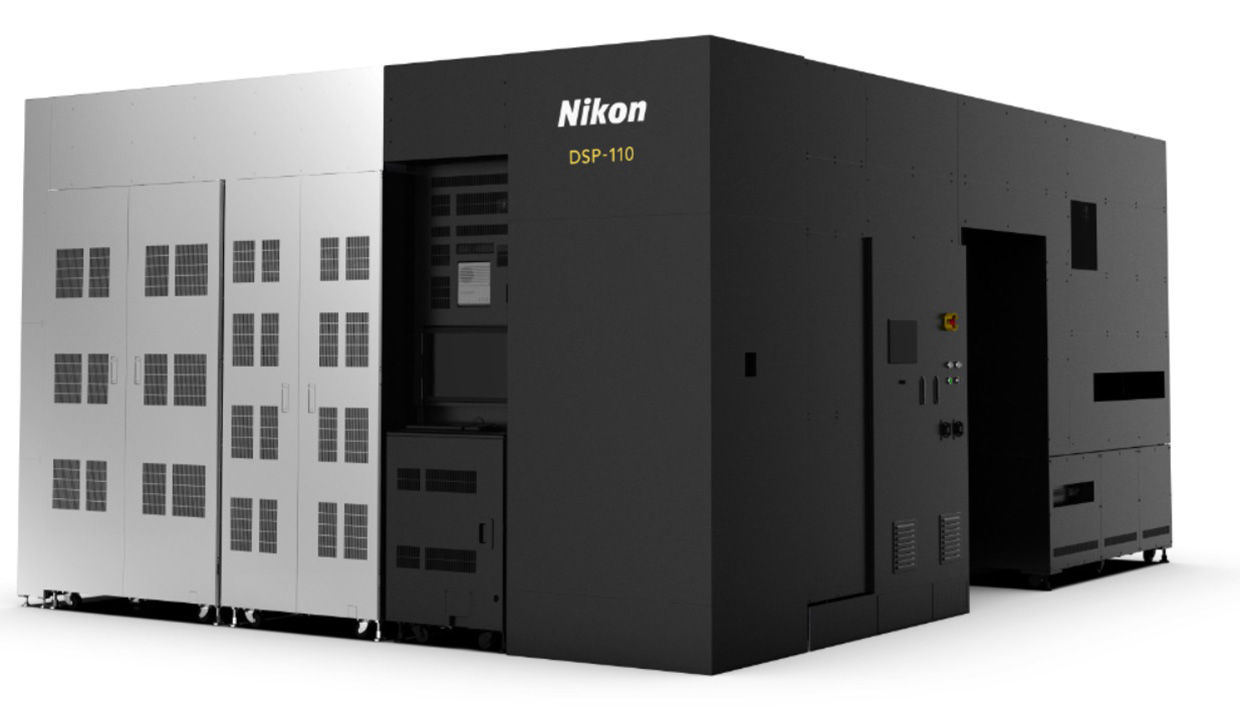
Nikon Corporation will release the DSP-110 digital lithography system for semiconductor advanced packaging in April 2027, featuring 1.5 µm resolution *1 (L/S *2) and throughput of 72 panels / hour *3. The DSP-110 also supports large substrates and achieves approximately 40% higher throughput than the DSP-100, which offers resolution of 1.0 µm (L/S) *4.
*1: 1 µm (micrometer) represents one-millionth of a meter (one-thousandth of a millimeter).
*2: Abbreviation for Line and Space. Refers to the width of circuit lines and the spacing between adjacent patterns.
*3: Based on 510 × 515 mm substrates
*4: July 16, 2025 press release: https://www.nikon.com/company/news/2025/0716_01/
In the semiconductor advanced packaging market, the importance of redistribution layer (RDL) patterning technology is increasing, driven by growing demand for high-density wiring for large interposers and multilayer FC-BGA substrates *5.
Nikon has been developing digital lithography systems that eliminate the need for photomasks while achieving both high resolution and high productivity. Nikon is launching the DSP-110 with 1.5 µm (L/S) resolution as a successor following the DSP-100 with 1.0 µm (L/S) resolution. The improved throughput of the DSP-110 was achieved by redesigning the optical system of the DSP-100. This was made possible by Nikon’s unique technological capabilities in designing and manufacturing optical systems in-house. Going forward, Nikon will continue to closely monitor technology trends in advanced packaging while responding to customers’ diverse needs, including resolution and supported substrate types.
*5: FC-BGA is an abbreviation for Flip Chip-Ball Grid Array. It refers to a high-density semiconductor package substrate that enables higher speed and more functionality in Large-scale Integration (LSI) chips.
Product name Digital lithography system DSP-110
Resolution 1.5 µm L/S
Light Source Equivalent to i-line
Overlay Accuracy ≦± 0.3 µm
Supported substrate sizes Square substrates: 310 × 310 mm, 510 × 515 mm, 600 × 600 mm, 730 × 920 mm, and others Wafers: 300 mm and others
Throughput 72 panels/hour (for 510 × 515 mm substrates)
Scheduled Release April 2027
By redesigning the optical system for 1.5 µm (L/S) resolution, throughput has been improved by approximately 40% compared to the DSP-100. In addition to maintaining high overlay accuracy of ≦± 0.3 µm, the DSP-110 achieves a throughput of 72 panels per hour *3. This contributes to improved productivity and reduced total costs for customers.
2. Expanded Focus Margin *6Through redesign of the optical system, the focus margin has been expanded compared to the DSP-100. This enables stable patterning across diverse substrate conditions, contributing to improved yield and mass production stability.
*6: The tolerance range within which accurate circuit dimensions can be maintained even when the focal point is shifted.
As advanced packaging technology continues to evolve, lithography systems for RDL are expected to require even higher resolution. The DSP-110 can be upgraded to achieve a resolution of 1.0 µm (L/S) by replacing its optical system, allowing flexible support for customers’ future process advancements.
The information is current as of the date of publication. It is subject to change without notice.
( Press Release Image: https://photos.webwire.com/prmedia/8/362788/362788-1.jpg )
WebWireID362788
This news content was configured by WebWire editorial staff. Linking is permitted.
News Release Distribution and Press Release Distribution Services Provided by WebWire.