Canon commences sales of FPA-3030i5a Semiconductor Lithography System supporting reduced cost of ownership manufacturing for small substrates
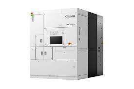
Canon Inc. announced today the launch in Japan of the FPA-3030i5a, the newest entry in the companys lineup of i-line1 stepper semiconductor lithography systems that support the manufacture of such devices as compound semiconductors and reduce cost of ownership (CoO), an indicator of the total cost required for semiconductor manufacturing.
The FPA-3030i5a semiconductor lithography system is designed to process small substrates of 8 inches or less, and supports not only silicon wafers, but also compound semiconductor materials such as SiC (silicon carbide) and GaN (gallium nitride). This helps make possible the manufacture of various semiconductor devices that are expected to see increased demand in the future, including high-power devices for automobile electrification and high-bandwidth devices for 5G communication. In addition, the hardware and software have been upgraded from those of the systems predecessor model, the FPA-3030i5+ stepper (released in June 2012), helping to reduce CoO.
The FPA-3030i5a employs a feeder system capable of handling a variety of wafer materials and sizes, including compound semiconductors with a diameter from 2 inches (50 mm) to 8 inches (200 mm). In addition, thanks to a new off-axis alignment scope to illuminate and measure wafer alignment marks without passing through a projection lens, the system makes possible alignment measurement at a wide range of illumination wavelengths.
Backside alignment, or Through Silicon Alignment (TSA) is also available as an option to adapt a variety of customer manufacturing processes. The FPA-3030i5a also inherits the imaging performance of its predecessor model, achieving exposure resolution of 0.35 micrometer2 line width patterns. Through the implementation of these functions, system owners are able to manufacture specialty power and communication devices using a wide range of wafer materials including compound semiconductors such as SiC.
By adopting such hardware as a new alignment scope that shortens the measurement time of alignment marks and a high-speed feeder system, as well upgraded software, the FPA-3030i5a achieves 123 wafers per hour (wph), an approximately 17% improvement in productivity compared with its predecessor model. In addition, by changing the chamber temperature control system, which maintains the lithography system in a clean environment and constant temperature, reducing power consumption by approximately 20% compared to the FPA-3030i5as predecessor model. Through such improvements, the system helps meet the needs of users seeking reduced CoO.
The FPA-3030i5a will go on sale in Japan in early March 2021.
1 A semiconductor lithography system that utilizes a 365 nm wavelength mercury lamp as the light source. 1 nm (nanometer) is 1 billionth of a meter.
2 1 micrometer is 1 million times 1 meter (= 1000/1mm).
The total cost required for capital investment and operation of a semiconductor manufacturing system. This is one of the indicators of the productivity of the manufacturing system and its processes on the mass production and is taken into consideration by manufacturers when selecting equipment.
Lineup of semiconductor lithography systems for small substratesCanons lithogaphy systems for small substrates support not only silicon wafers, but also compound semiconductor wafers, which comprise a variety of small wafers. The companys current lineup consists of three products: the KrF excimer laser stepper3 FPA-3030EX6 (released in July 2016) serves users who require high resolution.; the i-line stepper FPA-3030iWa (released in February 2020) supports a wide exposure range and uses a projection lens with a variable NA (numerical aperture) from 0.16 to 0.24, which ensuring high DOF (depth of focus) to make possible exposure with high accurcy and uniformity.
3 The exposure wavelength is 248nm. The semiconductor lithography system that uses the laser light generated by mixing krypton (Kr) gas, a rare gas, and fluorine (F) gas, a halogen gas.
Market trends in semiconductor lithography systemIn recent years, with the rapid development of the Internet of Things (IoT), the use of wafers of materials and sizes suitable for various devices is increasing along with the demand for such IoT technologies as communication devices and power devices. Semiconductor lithography systems are necessary to support specialized and small substrates, including compound semiconductor wafers and small wafers made from SiC, GaN and silicon.
(Based on Canon research)
For detailed product specifications, please refer to our website.
The Canon Lithography System 50-year anniversary websiteThis year marks the 50th anniversary of Canons full-scale entry into the lithography system business. To commemorate the occasion, Canon has published the Canon Lithography Equipment 50th Anniversary website, which features easy-to-understand explanations, including illustrations and videos, of the technologies behind semiconductor lithography, as well as a dedicated page for kids.
URL: https://global.canon/en/product/indtech/semicon/50th/anniversary/
( Press Release Image: https://photos.webwire.com/prmedia/6/265766/265766-1.jpg )
WebWireID265766
This news content was configured by WebWire editorial staff. Linking is permitted.
News Release Distribution and Press Release Distribution Services Provided by WebWire.